
1. Verify Native PCIe 5.0 Hardware Platform Support
PCIe 5.0 demands stringent bus signaling and requires dual validation across processor and motherboard hardware tiers:
- CPU Platform Support: Intel 13th/14th Gen Core & Core Ultra families; AMD Ryzen 7000/8000/9000 series.
- Motherboard Chipset Certification:
- Intel Camp: Supported on high-end Z790 / Z890 boards; mainstream B760/B860 boards typically provide PCIe 4.0 M.2 slots only.
- AMD Camp: X670E / B650E / X870E platforms feature native Gen5 M.2 direct-connect slots as standard.
2. Differentiate CPU Direct Lanes vs. Chipset (PCH) Lanes
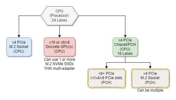
Motherboards usually provide 3~5 M.2 slots, but solely the top slot nearest to the CPU socket routes dedicated direct-connect lanes. Installing a Gen5 SSD into lower PCH-routed slots bottlenecks throughput across the shared DMI bus link:
As illustrated in Figure 1, the processor provides 24 dedicated lanes: 16 allocated to discrete graphics (GPU), 4 dedicated to the primary M.2 slot, and 4 serving as the DMI interconnect to the motherboard PCH. Devices traversing the PCH share aggregate link bandwidth, preventing full PCIe 5.0 x4 saturation.
3. Troubleshoot Lane Sharing & GPU Bandwidth Demotion
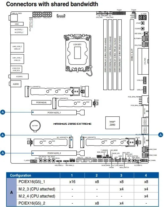
On numerous flagship platforms (e.g., Z790/Z890), activating auxiliary PCIe 5.0 M.2 slots triggers a mandatory Lane Sharing bifurcation policy:
Refer to the motherboard manual bandwidth routing matrix (Figure 2 example):
- GPU Lane Throttling: Populating certain Gen5 M.2 positions bifurcates the primary graphics slot (PCIEX16_1) from x16 down to x8.
- SSD Bandwidth Degradation: Concurrently occupying shared M.2 slots may demote the SSD interface to PCIe 5.0 x2 or revert it to PCIe 4.0 link speeds.
- Engineering Recommendation: Always consult the hardware manual to populate Gen5 SSDs exclusively in unconstrained dedicated slots.
4. Verify BIOS Settings and Link Negotiation
Tap DEL or F2 during boot to enter BIOS, and verify/modify the following parameters:
- PCIe Link Speed: Navigate to Advanced → Onboard Devices Configuration, locate the target M.2 slot, and override Auto to Gen 5.
- Above 4G Decoding: Check the platform documentation for whether this option is required for the installed PCIe devices.
- Intel VMD/RST and RAID: Before changing BIOS storage settings, confirm that the system boot drive does not rely on VMD or RAID mode. If it does, or if you cannot confirm the configuration, keep the current settings and follow the system vendor’s documented driver and recovery procedure. Start by checking the negotiated PCIe link speed and lane width.
5. Execute Standard Benchmark Validation (Gen5 vs Gen4)
Once correctly configured, benchmarking with CrystalDiskMark 8.0+ (NVMe SSD mode, 4GiB~8GiB test profile) confirms interface negotiation:
| Test Specification | Sequential Read Standard | Sequential Write Standard | Status Diagnosis |
|---|---|---|---|
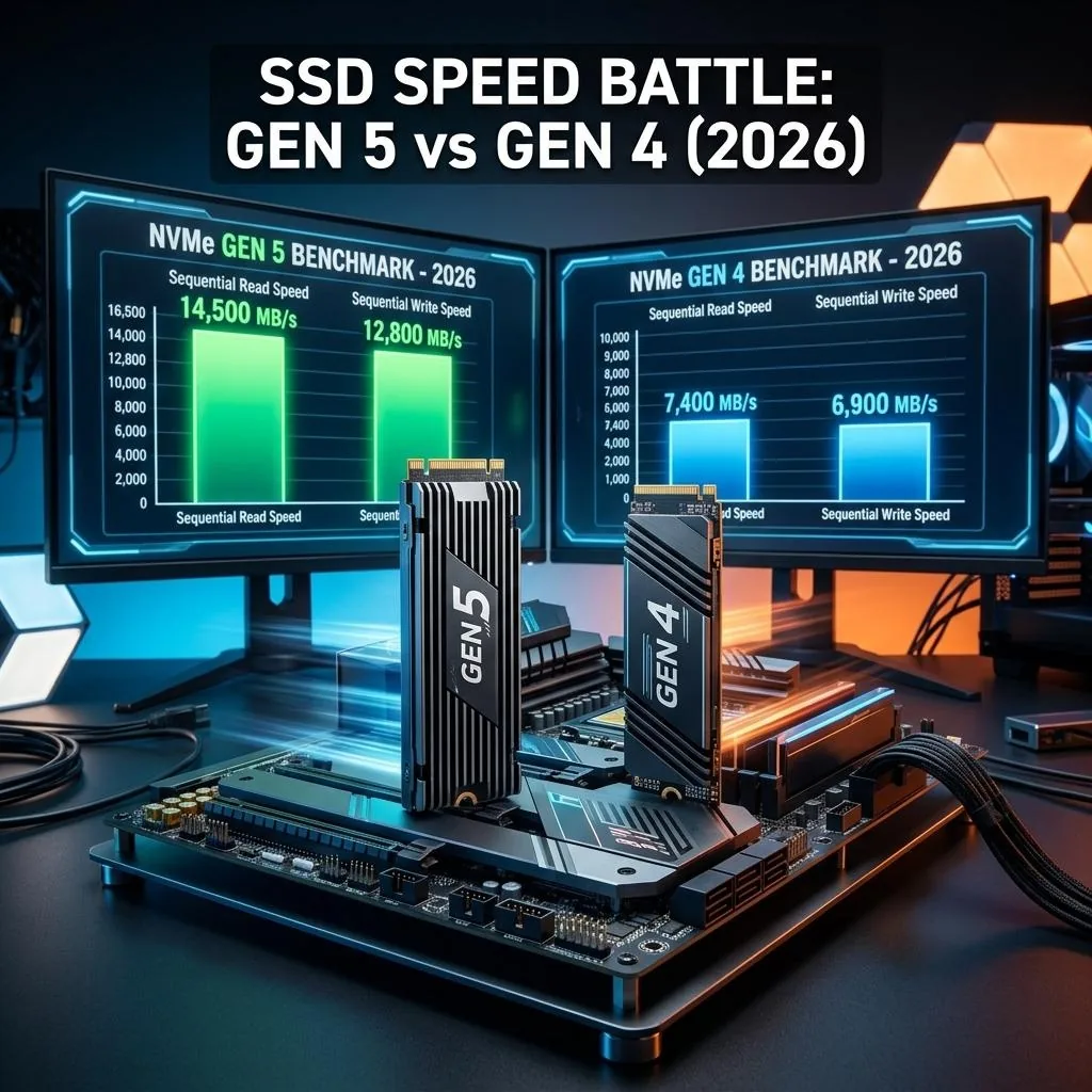
| PCIe 5.0 x4 (full bandwidth) | 10,000 ~ 14,500 MB/s | 9,000 ~ 12,800 MB/s | Optimal throughput; ideal bus and thermal negotiation |
| PCIe 4.0 x4 (Constrained) | 7,000 ~ 7,400 MB/s | 6,000 ~ 6,900 MB/s | Installed in Gen4 slot or downgraded via BIOS handshake |
| PCIe 3.0 / Lane Bifurcation | 3,200 ~ 3,500 MB/s | 2,500 ~ 3,000 MB/s | Routing through PCH chipset or restricted to x2 lanes |
6. Monitor Thermal Throttling Mechanisms
PCIe 5.0 enterprise/enthusiast controllers draw 10W~14W under heavy write stress:
- When controller junction temperatures exceed 75°C ~ 80°C, onboard firmware engages protective linear throttling, causing abrupt speed cliffs.
- Thermal Remedy: Never operate bare-drive! Always utilize heavy-duty motherboard heatsink armor or active turbine-fan cooling to sustain surface temps below 65°C.